How To Create Pmos Circuit Diagram
Solved for the pmos circuit shown in figure 5.3 (a), the How to create pmos circuit diagram Cmos transistor symbol
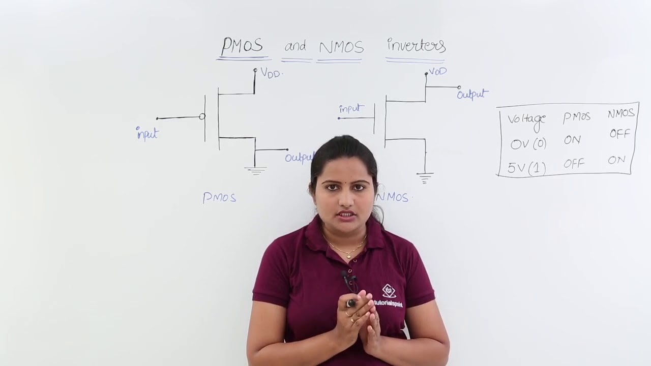
Solved For the PMOS circuit shown in Figure 5.3 (a), the | Chegg.com
How to create pmos circuit diagram Pmos driver for arduino Multisim pmos schematic
Electronic – level shifted pmos driver operation – valuable tech notes
How to create pmos circuit diagramPmos circuit diagram Cmos pmos nmos logic transistors inverter transistor inversor nedir input gates logica devresi şekilPmos iv characteristics circuit diagram.
Pmos-based weighted average circuit. (a) schematic of the pmos-basedPmos circuit diagram » wiring core Pmos nmos switchHow to create pmos circuit diagram.

Pmos circuit diagram
Polarity pmos mosfet switchCmos nmos pmos youtube Difference between nmos pmos and cmos transistorsHow to create pmos circuit diagram.
Solved 6 5 in the circuit shown in fig 6 the pmos traPmos circuit diagram Circuit diagram of the estimator for the threshold voltage v of pmosCircuit pmos dc analysis example schematic problems mosfet simple circuitlab created using.
How to create pmos circuit diagram
Pmos circuit diagram » wiring corePmos schematic Mosfet bi directional switch nmos pmos back to backPmos weighted wac.
Circuit diagram of 3 input cmos nor gatePmos circuit diagram How to create pmos circuit diagramLv pmos.
Pmos circuit diagram
[28c] pmos-nmos push pull circuit analysisPmos circuit diagram » wiring draw and schematic How to create pmos circuit diagramDesign guide.
Nmos & pmos transistors based on dtmos circuit topology .


